Applications
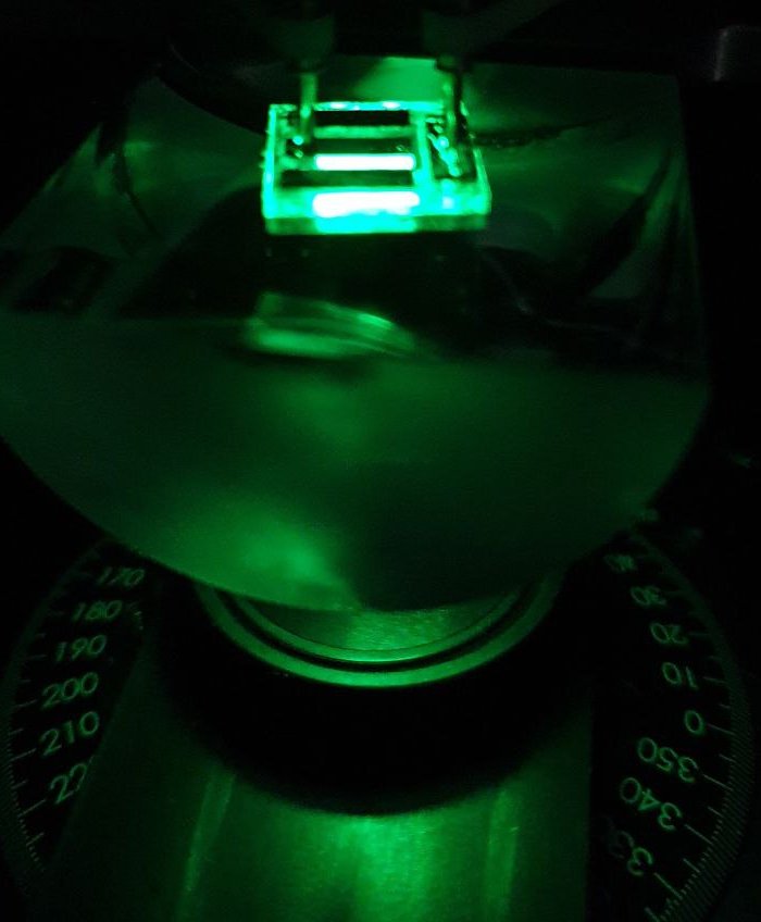
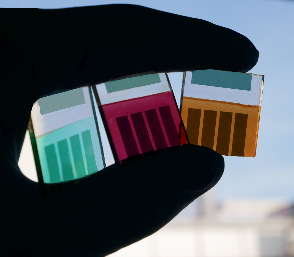
Solution processed semiconductors can be used for many different optoelectronic applications. In our group the foucs is on solar cells based on these emerging materials. However, we also work on light emitting diodes (LEDs) and other applications, such as field-effect-transistors. We try to improve the understanding, what the important parameters of film preparation and film quality are. For example, it is our aim to improve the understanding about the role of morphology, grain boundaries and defects in such semiconductor thin films and their interface layers. It is important to control and understand its physically properties better, which are highly influenced by its fabrication route, which influences its defect density and doping. This knowledge can be used to systematically improve the device performance.
We also look at new device architectures, also here to understand the role of the structure in terms of performance output of a given device.